Electronihack

Thursday, June 10, 2010

Process "hangs" for 6-8 seconds

I'm running in to some weird issues with a custom caching system I've built. I have 5 computers running a test client, hitting my server (across WCF) with about 40 threads each. For the full test they make 1000 calls per thread. The call they are making isn't overly complex -- it grabs small amounts of data from about 8-10 large dictionaries then combines the data into result rows and returns a max of 30 rows. The complete round trip time of the call (when called singly) is about .3 seconds.

With 5 clients (200 threads total) hitting the server at once, the 8 CPUs sit at about 50% usage each. The response times have grown anywhere from 2-4 seconds for each client. Not really great, but I'll deal for now.

After about 30 seconds or so, all 8 CPUs drop to 0% and stay there for about 8-10 seconds. This obviously causes the response times to shoot way up (around 15 seconds or so; depends on how long it's hung). The CPUs then pick back up and everything resumes as usual. This doesn't just happen once near the beginning. It happens multiple times during the test with no certain frequency.

Something else that is puzzling is that after one of these big "hangs", the base line processor usage jumps to about 65%. When that happens, response times start jumping all over the place. I'll see some that are 2 seconds, others that are closer to 20 seconds!

After some time, the baseline usage will come back down closer to 40-50%, where response times level back out around 2-4 seconds. Then it all happens again.

I'm putting together some screen shots of processor usage and such. I will be posting those shortly. I'll be posting some graphs from perfmon, so if you have any advice on which counters would be most helpful to see here, please let me know.

Host machine: Windows Server 2008 SP1 x64; Xeon W5590 @ 3.33GHz; 24GB RAM; 2 SSDs in RAID 0;

Client machines: Windows Vista Business SP1; Core2 Duo E8500 @ 3.16GHz; 8GB RAM;

Update:
I took a process dump during one of the bigger hangs. Here's what the stacks look like.


Processor graphs:
1) The first graph is at the very beginning of testing, after the clients had been running for a few seconds. Around 50% average load per processor.
2) The second graph was a "minor" hiccup. When it happened all the client response times spiked just briefly to around 15 seconds.
3) The third graph was really bad. All the clients "hung", then reported response times of near 20 seconds. This happened for around 8-10 seconds.
4) After the terrible "hang" earlier, everything started responding again. You can definitely tell that the CPU usage ended up well above where it started. Response times around this time are all over the place, from 2 to 20 seconds.

"Processor affinity" when making WCF calls from multiple threads

I'm having a strange problem with my WCF client/server. From a "fresh" client I fire off 100 calls from a single thread and my server processes all the calls on a single processor. Great. From a fresh client again, I fire off 100 calls from 10 threads (10 each), it still processes them all on one processor. However, if I start a fresh client and fire off 100 calls on one thread then immediately follow that by 100 calls over 10 threads, I see all 8 processors handling calls.

Fresh client:
100 calls from 1 thread on client puts all calls on only 1 logical processor on server

Fresh client:
10 calls from 10 threads on client puts all calls on only 1 logical processor on server

Fresh client:
100 calls from 1 thread on client immediately followed by
100 calls from 10 threads on client puts calls successfully on ALL 8 logical processors on server

So why does a fresh client's calls always get serviced by a single logical processor? Why does the second set of calls get serviced by all logical processors?

Sample code from client:
public partial class MyAgentClient
{
    static System.ServiceModel.Channels.Binding _binding;
    static System.ServiceModel.EndpointAddress _endpoint;
    static ChannelFactory<IMyAgent> _channelFactory;
    static IMyAgent _channel;

    static MyAgentClient _instance;
    public static MyAgentClient Instance
    {
        get
        {
            return _instance;
        }
    }

    static MyAgentClient()
    {
        _binding = WCFSettings.CurrentBinding;
        _endpoint = new EndpointAddress(WCFSettings.CurrentURI + "/MyAgent");
        _instance = new MyAgentClient();
        _channelFactory = new ChannelFactory<IMyAgent>(_binding, _endpoint);
        _channel = _channelFactory.CreateChannel();
    }

    public MyReturnData GetSomeData(string p1, string p2, string p3, SomeEnum p4, int p5, int p6)
    {
        try
        {
            return _channel.GetSomeData(p1, p2, p3, p4, p5, p6);
        }
        catch (Exception ex)
        {
            // Log the exception.
        }
    }
}
Sample code from server:
[ServiceContract]
public interface IMyAgent
{
    [OperationContract]
    MyReturnData GetSomeData(string p1, string p2, string p3, SomeEnum p4, int p5, int p6);
}

[ServiceBehavior(ConcurrencyMode = ConcurrencyMode.Multiple, InstanceContextMode = InstanceContextMode.PerCall, UseSynchronizationContext = false)]
public class MyAgent : IMyAgent
{
    public MyReturnData GetSomeData(string p1, string p2, string p3, SomeEnum p4, int p5, int p6)
    {
        try
        {
            return MyCode.StaticMethods.GetSomeData(enterpriseCode, companyNumber, salespersonFilter, leadCategoryType, startIndex, pageSize);
        }
        catch (Exception ex)
        {
            // Log the exception.
        }
    }
}
WCF binding:
public static CustomBinding NewTcpBinding
{
    get
    {

        TimeSpan oneMinute = new TimeSpan(0, 1, 0);
        TimeSpan tenMinutes = new TimeSpan(0, 10, 0);

        ReliableSessionBindingElement reliableSession = new ReliableSessionBindingElement();
        reliableSession.MaxPendingChannels = 512;
        reliableSession.Ordered = false;
        reliableSession.FlowControlEnabled = false;
        reliableSession.MaxTransferWindowSize = 4096;
        reliableSession.InactivityTimeout = tenMinutes;

        BinaryMessageEncodingBindingElement binaryEncoding = new BinaryMessageEncodingBindingElement();
        binaryEncoding.ReaderQuotas.MaxStringContentLength = 2147483646;
        binaryEncoding.ReaderQuotas.MaxArrayLength = 50000000;

        TcpTransportBindingElement tcpTransport = new TcpTransportBindingElement();
        tcpTransport.MaxReceivedMessageSize = 2147483646;
        tcpTransport.MaxBufferSize = 2147483646;
        tcpTransport.MaxBufferPoolSize = 524288;
        tcpTransport.TransferMode = TransferMode.Buffered;

        BindingElementCollection elements = new BindingElementCollection();
        elements.Add(reliableSession);
        elements.Add(binaryEncoding);
        elements.Add(tcpTransport);

        CustomBinding binding = new CustomBinding(elements)
        {
            Name = "TcpBinding",
            CloseTimeout = oneMinute,
            OpenTimeout = oneMinute,
            ReceiveTimeout = tenMinutes,
            SendTimeout = oneMinute
        };
        return binding;
    }
}

Tuesday, December 16, 2008

Muxing Around

***Disclaimer***
I do not claim to be nor do I consider myself to be an electronics expert, guru, etc. I am simply a hobbyist with no formal EE (or the like) education. If I write something completely wrong, or it is apparent that I have no idea what I am talking about, please leave a comment and set me straight. I am merely documenting my experiences and discoveries as I progress through my projects.


A buddy of mine, Jeremy, asked me the other day if I could help him out with a multiplexer/de-multiplexer chip he purchased. He was having some issues with it and couldn't quite get the results he expected. Below are some of the details on how I got this chip to work.

First off, the chip is an HEF4051B by Philips. It is an 8 channel, 3-bit chip. It's simply meant as a way to control 8 I/O pins, one at a time, while only using 3-4 I/O pins on your microcontroller. I'm sure there are other really good reasons for the chip (I believe it might double as an ADC, but I'm not sure?), but that's the most apparent one at this point.

Jeremy is using this chip as part of a larger DIY pinball machine project. Hopefully he will post some more info about the machine on his blog. If I recall correctly, the LED panels (no, not LCD) he's creating for score keeping and such will be composed of around 8,000+ surface mount LEDs!

"What is he using this chip for in his pinball machine?", you may be asking. Well, it's definitely not to control the LEDs :P It's actually to control various inputs. It will be responsible for detecting inputs from the flippers, drop targets, etc.

So how does this chip actually get used? Well, as stated above, this chip connects to four pins on your microcontroller. Jeremy and I both just happen to be using the Parallax Propeller microcontroller (I have a whole series of blog posts I need to make on this microcontroller. I won't get into it here.). The Propeller has 32 I/O pins. If we connect 8 of these mux chips to the Propeller, we can effectively double the number of I/O pins on the microcontroller for just around $3 (there are many reasons for doing it this way, of which costs is probably the least important).

So this is a very simple schematic I whipped up in about 2 minutes. It shows how to connect the mux chip to the Propeller in order to run 8 LEDs on 4 microcontroller pins. I know, we aren't supposed to be running LEDs, we are supposed to be reading in switches. I just did it this way first, so I figured I'd post the schematic for it.


(P8X32A is the Propeller chip)

So how do we tell the mux chip which LED to turn on just by using 4 digital pins on the Propeller? Well, to be fair we only really use 3 pins when doing output (like we are doing right now). We use four pins to do input (when we use switches).

Okay, so from the schematic you will notice there are 7 I/O pins, labeled Y0 through Y7. To turn on the LED on pin Y5, we need to send "5" to the mux chip. We can't do that on just one pin, so we have to do it with the 3 pins (S0, S1 and S2 on the mux chip; P1, P2, and P3 on the Propeller). You have probably figured out by now how we do that. If not, here goes:

5 in binary is 101.
101 on the Propeller would be P1 = 1, P2 = 0, P3 = 1

We also have to set the Z pin on the mux chip to a high output (this is what the mux chip requires in order to do outputs to LEDs).

Here's the Spin code (Propeller programming language) I used:

CON
_clkmode = xtal1 + pll16x
_xinfreq = 5_000_000

mZ = 15 'common input/output
mS0 = 11 'select input
mS1 = 10 'select input
mS2 = 9 'select input

enabledLed = 0


PUB main
dira[enabledLed]~~
outa[enabledLed] := 1

dira[mZ]~~
outa[mZ] := 1

dira[mS0]~~ 'set to output
dira[mS1]~~ 'set to output
dira[mS2]~~ 'set to output

outa[mS0] := 1
outa[mS1] := 0
outa[mS2] := 1

repeat

Simple enough. Now, this is the schematic for doing the input with switches.


So really it's just about the same. We just have 5v switches that ground to Y0 through Y7 on the mux chip. So now all we have to do is read the value from the mux chip when a switch is pressed.

I originally though this part would be easy since the LED part was so easy. All I have to do is press a switch then read S0, S1 and S2 to get a binary value, right? Wrong! It doesn't work that way.

Let's say we want to check if switch #7 (Y7; it's actually the 8th switch) is pressed. We have to set S0..S2 to 111 (or 7), then read from Z to see if it's high or low (in this case, high is any voltage, low is 0 volts). This tells the mux chip you are interested in Y7, then the mux chip sets Z to the voltage coming in to Y7 through the switch, which can then be interpreted by the Propeller chip. Obviously we have to iterate over all 8 switches and check them individually, but that's okay -- we can do it really fast!

Here's some code:
CON
_clkmode = xtal1 + pll16x
_xinfreq = 5_000_000

mZ = 15 'common input/output
mS0 = 11 'select input
mS1 = 10 'select input
mS2 = 9 'select input

enabledLed = 0

PUB main
dira[enabledLed]~~

dira[mZ]~

dira[mS0]~~ 'set to output
dira[mS1]~~ 'set to output
dira[mS2]~~ 'set to output

repeat
outa[mS0] := 1
outa[mS1] := 1
outa[mS2] := 1

if(ina[mZ] == 1)
outa[enabledLed] := 1
else
outa[enabledLed] := 0
So I'm not actually iterating over all the switches, but you can change the code to do that if you want. All I'm doing is checking to see if the switch on Y7 is pressed. If it is, then I turn on an LED. If it isn't pressed, I turn off the LED. Very simple example, but it proves the concept. The main thing to not here is that the pin referenced by "mZ" has been set as an input rather than a high output. This allows us to read the pin after the mux chip sets it.

Please post comments if you have any questions.

Saturday, December 13, 2008

Do-It-Yourself PCB Manufacturing

Welcome to my first ever blog post! I intend to use this blog to follow the progress of my various robotics & automation projects. I currently have four projects that I am working on simultaneously, all of which require quite a bit of electronics.

Like most electronics hobbyists out there, I find myself making constant use of the breadboard. What makes me like breadboards so much is the same thing that keeps them from being good prototype/production circuit boards -- no soldering!

Of course, you can transfer your "breadboarded" circuit to a perfboard and solder everything together, but that too has its downsides -- lots of wire stripping and debugging, messy wires, etc.

I have found a process that works well for me:
  1. Design the schematic for the circuit using ExpressSCH (free!)
  2. Breadboard the circuit, debug, refactor schematic, rinse, repeat
  3. Design a PCB layout using ExpressPCB (free!)
  4. Manufacture the PCB and solder on the components for a complete board!
Now, #4 is obviously made up of quite a few steps (which is what this blog post is originally intended to detail). Below I will describe my process of doing this. The end result is a beautiful PCB, with little to no wires, which is basically just a real world manifestation of a "circuit model" drawn up on the computer. At least that's how I see it! :)

Manufacture the PCB

Step One, print the schematic on a transparency film. I used a HP LaserJet (don't recall the model # of my own printer) and laserjet transparency films from 3M. I paid $15.46, after shipping, for a pack of 50, or $0.31/sheet.


Step Two, expose your pre-sensitized PCB to UV light. The boards I bought came with instructions stating that I could expose them with just a 100 watt light bulb. I do not recommend this. UV light works MUCH better.

The board in its protective foil envelope:


I neglected to take a picture of the board after I took it out of the foil. Maybe next time. Anyhow, on to the exposing.

I placed the board on my counter top, aligned the transparency on top of the board just how I wanted it, then laid a 1/4" piece of Lexan (regular plate glass works fine too; steal some from a picture frame if you can't find a piece elsewhere around your house) on top to hold the artwork flat against the board.

Next, I laid a UV lamp on top of the Lexan and turned it on. The lamp I used was borrowed from my friend's lizard cage. It worked perfectly!


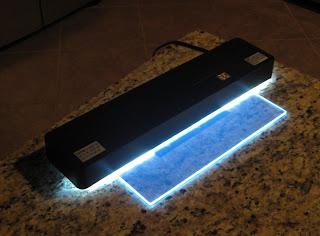
The exposing process looked pretty cool when I took a picture of it. I should probably recommend NOT staring at the lamp while it's on ;)

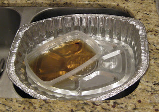
Step Three, develop the board! I had a leftover aluminum turkey roasting pan from Thanksgiving. I decided it was time to put it to use! I use the pan to simply hold hot water. I filled it with about 1-1/2" of hot water. Then I put a container of developer solution in the pan and let it float until the solution became quite warm.

Once the solution was warm, I switched off the UV lamp and threw the PCB directly into the developer bath. I agitated the board with my gloved fingers while it exposed. It took about 1-2 minutes for it to fully develop.

When the board was done developing I immediately dunked it into a big container of COLD water to stop further developing. I try not to run my boards under cold water coming straight from the faucet because it is bad practice to get these chemicals in your sink. If your sink is stainless steel (and it probably is), then it's REALLY bad practice to get the chemical from the next step in your sink. It will start to eat the metal in your sink. This is the same reason I let the developer solution float in a tray of hot water and not float directly in a sink of hot water.


The board after developing and a bath in cold water:


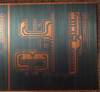
The dark color is the resist substance. It is the positive from my artwork. The area on the transparency that was black (my design) is now protected from the etchant solution in the next step. The exposed copper will shortly be eaten away, leaving a pretty circuit :)

Step Four, etch the board! I use a mixture four parts ferric chloride (FeCl) and one part tap water. I think my final solution was about 5-6 cups FeCl. As with the developer solution, FeCl works best when warm. The chemical reaction during the etching process actually cools down the solution, so I try to keep it warm throughout the whole process.

I found a large Rubbermaid container with a screw top lid that works great for this. It has a large opening in the top so I can reach my hand in and remove the PCB easily. With the container of FeCl sealed, I placed it in a sink of hot water for about 10 minutes. I then dropped the developed board into the FeCl. Constant agitation of the board definitely makes the etching process go much faster. After I put the board in, I resealed the container then constantly shook it around for about 5-7 minutes.

I pulled the board out and dropped it straight into the container of cold water I used after developing. This washed all the FeCl off just fine. At this point the remaining copper is still covered in the resist material. A little nail polish remover and a couple swipes with a paper napkin is all it takes to get rid of that.

The board after etching and acetone:


Step Five, tin the copper. This allows for much easier soldering and I guess it protects the copper from oxidation. I mixed up a bath of tinning solution and submerged the board for about 2 minutes. Around 2 minutes I looked at the board and it had a brilliant tin color and it was super glossy looking. It looked great! Unfortunately I followed the instructions on the tinning solution and left the board in for 15 minutes (which only ended up being half of the required 30 minutes), which was apparently WAY too long. The solution started damaging the finish. It's okay though, I know for next time :)

The board after tinning:


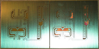
The board on the right looks a little funny because it didn't finish etching. That's okay because I only needed one of them.

After this I took the board to my drill press and drilled out all the holes with some super tiny PCB drill bits. Then I soldered it up and it worked PERFECTLY! Well, almost perfectly. If you spot the "T" on the left board, you'll see what I mean. That should've been connected to the ground plane but wasn't, so I just soldered the jumper.

Overall, this process is WAY easier than soldering up a perfboard. I can diagnose most issues through the schematic before I even make the PCB. After the PCB is designed in ExpressPCB, the whole process takes about 45 minutes to go from printout to drill press.